DS07-12517-2E
FUJITSU SEMICONDUCTOR
DATA SHEET
8-bit Proprietary Microcontroller
CMOS
F
2
MC-8L MB89628R/629R/P629
MB89628R/629R/P629
s
DESCRIPTION
The MB89628R/629R/P629 have been developed as a general-purpose version of the F
2
MC*-8L family
consisting of proprietary 8-bit, single-chip microcontrollers.
In addition to the F
2
MC-8L CPU core which can operate at low voltage but at high speed, the microcontrollers
contain a variety of peripheral functions such as timers, serial interfaces, an A/D converter, and an external
interrupt.
The MB89628R/629R/P629 are applicable to a wide range of applications from welfare to industrial equipment,
including portable devices.
*: F
2
MC stands for FUJITSU Flexible Microcontroller.
s
FEATURES
� Large-size RAM
MB89P629: 4 Kbytes
MB89628R: 3 Kbytes
MB89629R: 3 Kbytes
� High-speed processing at low voltage
Minimum execution time: 0.4
�
s/3.5 V, 0.8
�
s/2.7 V
� F
2
MC-8L family CPU core
Instruction set optimized for controllers
(Continued)
s
PACKAGE
Multiplication and division instructions
16-bit arithmetic operations
Test and branch instructions
Bit manipulation instructions, etc.
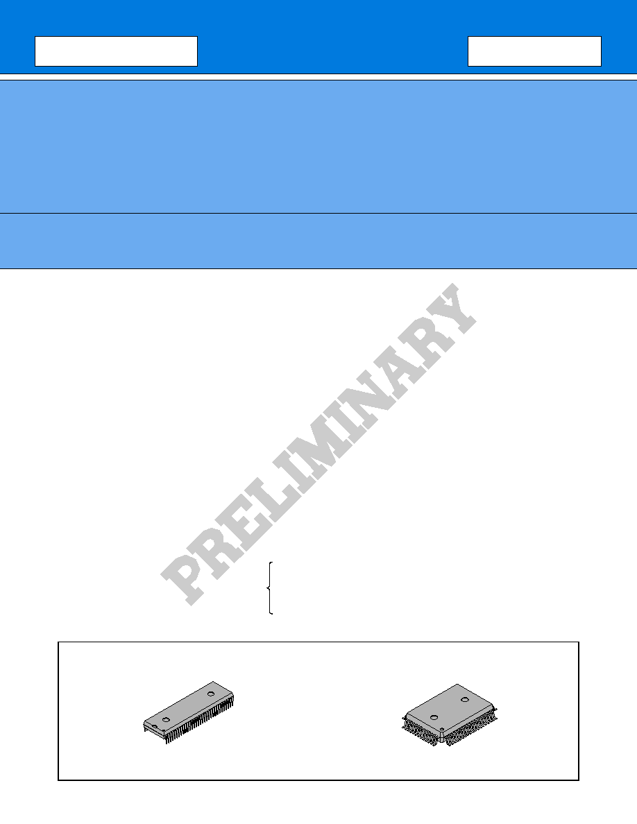
(FPT-64P-M06)
(DIP-64P-M01)
64-pin Plastic SH-DIP
64-pin Plastic QFP

2
MB89628R/629R/P629
(Continued)
� Four types of timers
8-bit PWM timer (also usable as a reload timer)
8-bit pulse width count timer (Continuous measurement capable, applicable to remote control, etc.)
16-bit timer/counter
20-bit time-base timer
� Two serial interfaces
Swichable the transfer direction allows communication with various equipment.
� 8-bit A/D converter
Sense mode function enabling comparison at 5
�
s
Activation by an external input capable
� External interrupt: 4 channels
Four channels are independent and capable of wake-up from low-power consumption modes (with an edge
detection function).
� Low-power consumption modes
Stop mode (Oscillation stops to reduce the current consumption.)
Sleep mode (The CPU stops to reduce the current consumption to approx. 1/3 of normal.)
3
MB89628R/629R/P629
s
PRODUCT LINEUP
*1: The piggyback/evaluation product is applicable to the MB89620 series.
*2: Varies with conditions such as the operating frequency. (See section "
s
Electrical Characteristics.") In the case
of the MB89PV620, the voltage varies with the restrictions of the EPROM for use.
MB89629R
MB89P629
MB89PV620
*1
Classification
Mass production products
(mask ROM products)
One-time PROM
product for evaluation and
development
Piggyback/evaluation
product for evaluation and
development
ROM size
24 K
�
8 bits
(internal mask ROM)
32 K
�
8 bits
(internal mask ROM)
32 K
�
8 bits
(internal PROM, programming
with general-purpose EPROM
programmer)
32 K
�
8 bits
(external ROM)
RAM size
3072
�
8 bits
4096
�
8 bits
1 K
�
8 bits
CPU functions
Number of instructions:
136
Instruction bit length:
8 bits
Instruction length:
1 to 3 bytes
Data bit length:
1, 8, 16 bits
Minimum execution time:
0.4
�
s/10 MHz
Interrupt processing time:
3.6
�
s/10 MHz
Ports
Input ports:
5 (4 ports also serve as peripherals.)
Output ports (N-ch open-drain):
8 (All also serve as peripherals.)
I/O ports (N-ch open-drain):
8 (4 ports also serve as peripherals.)
Output ports (CMOS):
8
I/O ports (CMOS):
24
Total:
53
8-bit PWM timer
8-bit reload timer operation (toggled output capable, operating clock cycle: 0.4
�
s to 3.3 ms)
8-bit resolution PWM operation (conversion cycle: 102
�
s to 839 ms)
8-bit pulse width count
timer
8-bit timer operation (overflow output capable, operating clock cycle: 0.4 to 12.8
�
s)
8-bit reload timer operation (toggled output capable, operating clock cycle: 0.4 to 12.8
�
s)
8-bit pulse width measurement operation (Continuous measurement "H" pulse width/"L"
pulse width/from
to
/from
to
capable)
16-bit timer/counter
16-bit timer operation (operating clock cycle: 0.4
�
s)
16-bit event counter operation (Rising/falling/both edges selectability)
8-bit serial I/O 1,
8-bit serial I/O 2
8-bits
LSB first/MSB first transfer selectability
One clock selectable from four transfer clocks
(one external shift clock, three internal shift clocks: 0.8
�
s, 3.2
�
s, 12.8
�
s)
8-bit A/D converter
8-bit resolution
�
8 channels
A/D conversion mode (conversion time: 18
�
s)
Sense mode (conversion time: 5
�
s)
Continuous activation by an external activation or an internal timer capable
Reference voltage input
External interrupt
4 independent channels (edge selection, interrupt vector, source flag)
Rising edge/falling edge selectability
Used also for wake-up from stop/sleep mode. (Edge detection is also permitted in stop mode.)
Standby modes
Sleep mode, stop mode
Process
CMOS
Operating voltage
*2
2.2 V to 6.0 V
2.7 V to 6.0 V
EPROM for use
MB89628R
MBM27C256A-20
Part number
Parameter
4
MB89628R/629R/P629
s
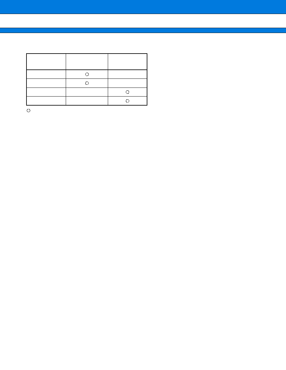
PACKAGE AND CORRESPONDING PRODUCTS
: Available
�
: Not available
Note: For more information about each package, see section "
s
Package Dimensions."
s
DIFFERENCES AMONG PRODUCTS
1. Memory Size
Before evaluating using the piggyback product, verify its differences from the product that will actually be used.
Take particular care on the following points:
� On the MB89P629, the program area starts from address 8007
H
but on the MB89PV620, MB89628R, and
MB89629R starts from 8000
H
. (On the MB89P629, addresses 8000
H
to 8006
H
comprise the option setting
area, option settings can be read by reading these addresses. On the MB89PV620, MB89628R, and
MB89629R, addresses 8000
H
to 8006
H
could also be used as a program ROM. However, do not use these
addresses in order to maintain compatibility of the MB89P629.)
2. Current Consumption
� In the case of the MB89PV620, add the current consumed by the EPROM which is connected to the top socket.
� When operated at low speed, the product with an OTPROM (one-time PROM) or an EPROM will consume
more current than the product with a mask ROM.
However, the current consumption in sleep/stop modes is the same. (For more information, see section
"
s
Electrical Characteristics".)
3. Mask Options
Functions that can be selected as options and how to designate these options vary by the product.
Before using options check section "
s
Mask Options."
Take particular care on the following points:
� A pull-up resistor cannot be set for P40 to P47 on the MB89P629.
� A pull-up resistor is not selected for P50 to P57 when the A/D converter is used.
� Options are fixed on the MB89PV620.
Package
MB89628R
MB89629R
MB89P629
MB89PV620
DIP-64P-M01
�
FPT-64P-M06
�
MDP-64C-P02
�
MQP-64C-P01
�
5
MB89628R/629R/P629
s
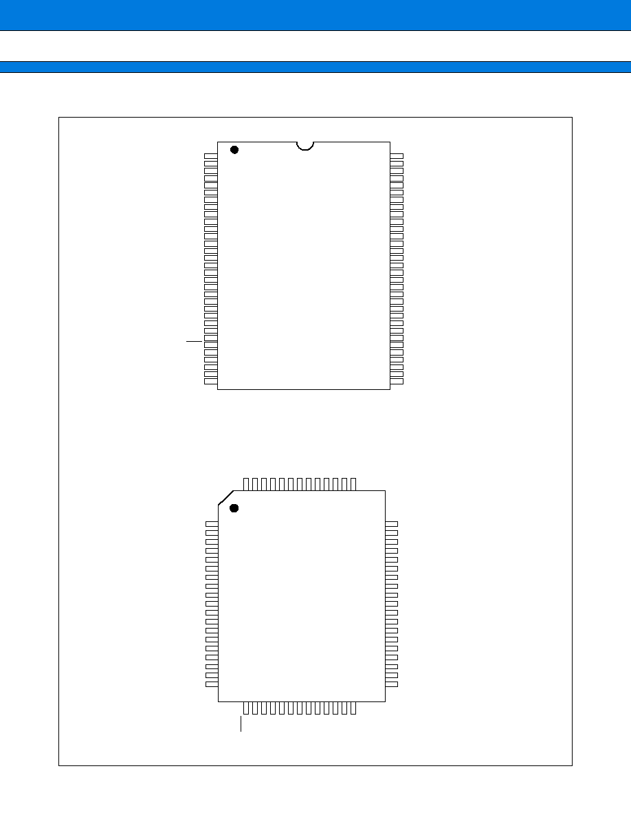
PIN ASSIGNMENT
(DIP-64P-M01)
(Top view)
1
P36/WTO
2
P37/PTO
3
P40
4
P41
5
P42
6
P43
7
P44/BZ
8
P45/SCK2
9
P46/SO2
10
P47/SI2
11
P50/AN0
12
P51/AN1
13
P52/AN2
14
P53/AN3
15
P54/AN4
16
P55/AN5
17
P56/AN6
18
P57/AN7
19
AV
CC
20
AVR
21
AV
SS
22
P60/INT0
23
P61/INT1
24
P62/INT2
25
P63/INT3
26
P64
27
RST
28
MOD0
29
MOD1
30
X0
31
X1
32
V
SS
V
CC
64
P35/PWC
63
P34/EC
62
P33/SI1
61
P32/SO1
60
P31/SCK1
59
P30/ADST/CLKO
58
V
SS
57
P00
56
P01
55
P02
54
P03
53
P04
52
P05
51
P06
50
P07
49
P10
48
P11
47
P12
46
P13
45
P14
44
P15
43
P16
42
P17
41
P20
40
P21
39
P22
38
P23
37
P24
36
P25
35
P26
34
P27
33
1
2
3
4
5
6
7
8
9
10
11
12
13
14
15
16
17
18
19
P45/SCK2
P46/SO2
P47/SI2
P50/AN0
P51/AN1
P52/AN2
P53/AN3
P54/AN4
P55/AN5
P56/AN6
P57/AN7
AV
CC
AVR
AV
SS
P60/INT0
P61/INT1
P62/INT2
P63/INT3
P64
51
50
49
48
47
46
45
44
43
42
41
40
39
38
37
36
35
34
33
P30/ADST/CLKO
V
SS
P00
P01
P02
P03
P04
P05
P06
P07
P10
P11
P12
P13
P14
P15
P16
P17
P20
64
63
62
61
60
59
58
57
56
55
54
53
52
P44/BZ
P43
P42
P41
P40
P37/PTO
P36/WTO
V
CC
P35/PWC
P34/EC
P33/SI1
P32/SO1
P31/SCK1
20
21
22
23
24
25
26
27
28
29
30
31
32
RST
MOD0
MOD1
X0
X1
V
SS
P27
P26
P25
P24
P23
P22
P21
(FPT-64P-M06)
(Top view)